The research activities of our group (Optical Spectroscopy of Nanostructured Materials laboratory) focus on the electronic properties of nanostructured semiconductor materials either spontaneously formed or artificially created.
To this end, we employ optical spectroscopy techniques based on photoluminescence (PL) and its variants (PL excitation, PL under magnetic field and other external perturbations), Raman scattering, and second order photon-correlation techniques.
Post-growth hydrogen irradiation is also employed as a powerful tool to fine tune the material electronic properties.
Highlights and News
March 2024
2D crystals feel the pressure . . . see how
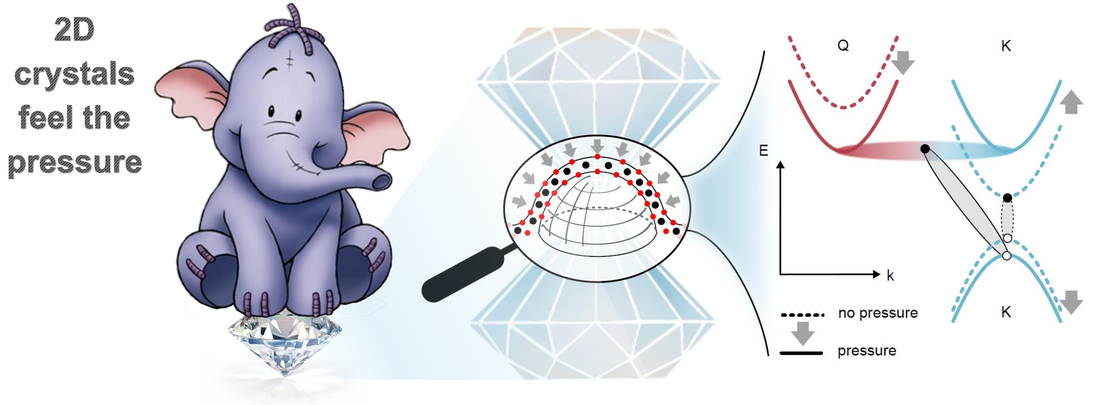
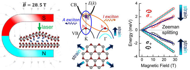
Two-dimensional (2D) crystals can be attained by exfoliation of van der Waals materials. The latter are formed by atomic layers held together by weak electrostatic forces, akin to graphene in graphite. Since the discovery of graphene twenty years ago, the number of 2D crystals has increased enormously, encompassing materials with metallic, insulating and semiconducting properties.
Semiconducting 2D crystals are particularly ripe with novel physical phenomena and great applicative prospects. Certainly, the success of a material system hinges on our capability to engineer its physical properties. In this respect, 2D materials and the corresponding physical properties can be widely modulated through various approaches that act directly on the band structure of the lattice, such as hetero-structuring, doping, alloying, the creation of defects, the application of electromagnetic fields, or mechanical deformations. Mechanical deformations rely on a change of the lattice structure by strain engineering (i.e., by stretching or compressing the crystal plane controllably) or by hydrostatic pressure. Indeed, mechanical tuning methods are uniquely efficacious in 2D semiconductors thanks to their all-surface nature and ensuing much stronger deformation capacity compared to covalently bound bulk lattices.
In a work published in Nano Letters [1], three young scientists of our Department, Elena Stellino and Beatrice D’Alò (at the HPS group, https://gruppohps.wordpress.com/) and Elena Blundo (at the OPERA group, https://antoniopolimeni-physics.weebly.com/), show that external hydrostatic pressure and morphological strain can be efficiently combined in transition metal dichalcogenide (TMD, such as MoS2 and WS2) 2D semiconductors. That approach, which represents a remarkable experimental challenge, has been rarely used despite its extremely insightful nature.
First, morphological strain was achieved by hydrogen irradiation of bulk WS2 that leads to the formation of hydrogen-filled, micrometer-sized, spherical bubbles made of a monolayer directly lifted from the underlying bulk lattice [2]. Owing to the membrane curvature and hydrogen internal pressure of tens to hundreds of atm, the monolayer experiences a biaxial tensile strain at the dome center (resulting in a record total strain of about 4%). Through a painstaking exfoliation and deposition procedure, the authors succeeded to place WS2 bubbles between the culets of a diamond anvil cell.
Secondly, exploiting the enormous force exerted by the diamond anvil cell culets, the authors applied a pressure in excess of 6000 atm on a monolayer bubble of WS2. That pressure corresponds to the pressure which would be applied by an adult elephant sitting on a 1 cm2 surface. Remarkably, the bubble withstood such a huge pressure and the modification of the crystal shape permitted a controlled modulation of the strain gradients at work on the system. By combining the results from micro-Raman and micro-photoluminescence experiments, the authors unveiled an anomalous pressure evolution of the band extremes in the conduction band (CB), responsible for the pronounced non-linearity observed in both the intensity and energy trend of the exciton band under pressure. A hybridization mechanism between distinct CB extremes was proposed. The crossover between different CB minima and their hybridization occurs at pressure values much lower than those predicted for planar monolayers, resulting in an exciton emission with a mixed direct/indirect nature and in-plane/out-of-plane orbital character.
The work frames a complete scenario for the pressure response of 2D crystals, which includes the evolution of their morphological features, lattice properties and electronic band structure and thus defines a new approach to investigate and, possibly, engineer the optoelectronic properties of 2D materials with prospects for pressure sensors.
[1] Elena Stellino, Beatrice D'Alò, Elena Blundo, Paolo Postorino, and A. Polimeni, Nano Lett. 2024; https://pubs.acs.org/doi/10.1021/acs.nanolett.4c00157
[2] E. Blundo et al., Phys. Rev. Lett. 127, 046101 (2021)
February 2024
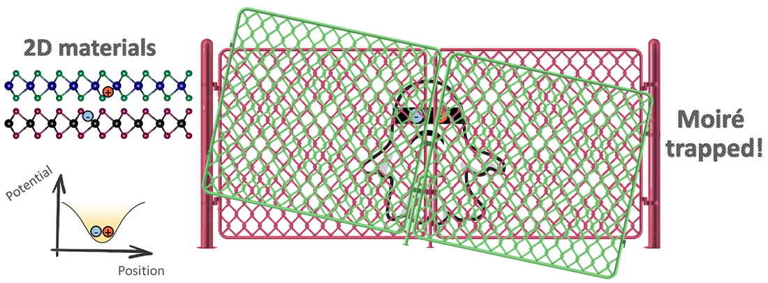
To moiré, or not to moiré, that is the question . . . and the answer can be found here
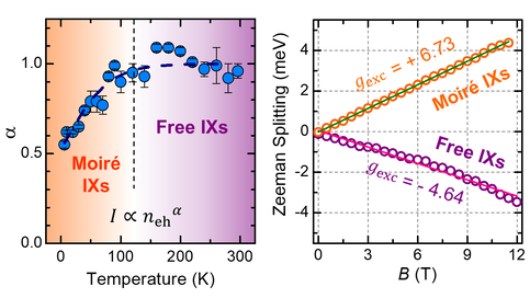 Left: Localised to delocalised transition of moiré excitons as deduced by the power law of the emission signal upon photogenerated exciton density.
Right: Evidence of the Localised to delocalised transition of moiré excitons from the sign reversal of the exciton moment.
Left: Localised to delocalised transition of moiré excitons as deduced by the power law of the emission signal upon photogenerated exciton density.
Right: Evidence of the Localised to delocalised transition of moiré excitons from the sign reversal of the exciton moment.
Two-dimensional (2D) crystals have led to a change of paradigm in Solid State Physics. The discovery of graphene, the forerunner of 2D crystals, dates back to 20 years ago. Since then, hundreds of 2D crystals have been isolated. The realm of Flatland comprises insulators, metals, semiconductors, superconductors, with unique electronic, optical, magnetic, transport, thermal, mechanical and catalytic properties that cannot be found in the material bulk counterpart.
Yet, the large interest of scientists for 2D crystals regards them not only as standing alone lattices, but also when combined as Lego bricks. Indeed, the all-surface nature of 2D crystals and the lack of lattice-matching constraints prompt the opportunity to stack different atomically thin planes into hetero-structures. The formation of 2D hetero-structures leads to engineerable chemical and physical properties, rich with surprising physical effects and applications.
A further boost to the creation of 2D hetero-structures comes from the possibility to play with the relative twist angle between the 2D lattices forming the hetero-structure that has led to the to emerging field of twistronics. Indeed, inherent to the stacking process is the formation of a twist angle-dependent moiré superlattice that superimposes on the topographic and electronic structure of the single 2D crystals. This phenomenon has been particularly investigated in hetero-structures made of semiconducting 2D materials, such as transition metal dichalcogenides, which feature a sizeable band gap and peculiar valley-spin properties. The moiré potential can be as deep as 100 meV and is able to trap excitons (electron-hole bound states) and other composite quasi-particles, such as trions and multi-excitons. Moiré-confined excitons (i.e. moiré excitons) are formed by charge carriers residing in the different layers of a hetero-structure. The space-indirect character of moiré excitons endows them with long lifetimes that, in conjunction with the depth of the moiré potential, make them suitable for the observation of high temperature (>100 K) Bose-Einstein condensates, exciton and Mott insulators, and Wigner crystals. Moiré excitons are also particularly interesting for quantum technologies as they can be exploited as nanoscale-ordered arrays of quantum emitters [1].
For boson condensates and highly correlated charge systems, as well as quantum photonics applications, the thermal stability of the moiré-induced confinement of the excitons plays a crucial role and a fundamental question arises: Up to what extent can moiré excitons be regarded as truly moiré-confined?
Elena Blundo and co-authors answer this crucial question in an article published in Nature Communications reporting temperature-/time- and magnetic field-dependent optical spectroscopy experiments on WSe2/MoSe2 2D hetero-structures [2]. The work led by the OPERA group (https://antoniopolimeni-physics.weebly.com/) at the Physics Department of Sapienza is the result of a collaboration with scientists at the CNR (Italy), Warsaw University (Poland) and NIMS institute (Japan). Elena Blundo et al. pinpoint the conditions under which excitons escape from the moiré potential by carefully investigating the effects of the temperature on the exciton: (i) emission lineshape (ii) temporal dynamics, and (iii) magnetic moment. Remarkably, exciton Zeeman splitting measurements up to 16 T unveils that the exciton magnetic moment reverses its sign when the moiré potential is not capable of localising excitons at elevated temperatures. In addition, the determination of the moiré exciton magnetic moment at different temperatures reveals for the first time the different symmetries of the moiré potential related to the local atomic registry of the hetero-structures.
These findings shed new light on the truly confined nature of the exciton states in a moiré superlattice with increasing temperature and exciton density, thus setting the conditions, e.g., for the observation and stability of nano-arrays of quantum emitters at elevated temperatures in moiré superlattices. The results demonstrate also how magnetic fields represent a valuable tool to determine the localised or delocalised status of charge carriers in 2D hetero-structures, which can be important for the understanding of fundamental effects, such as the formation of highly correlated electronic phases and boson condensation phenomena.
[1] L. Du et al., Moiré photonics and optoelectronics. Science 379, eadg0014 (2023).
[2] E. Blundo et al., Localisation-to-delocalisation transition of moiré excitons in WSe2/MoSe2 heterostructures, Nat. Commun. 15, 1057 (2024).
January 2024
Imaging the Quantum Capacitance of Strained MoS2 monolayers
We have investigated the electric field response of biaxially strained MoS2 monolayers (MLs) in the form of bubbles. These bubbles were produced via H-ion irradiation of bulk crystals. low energy treatments performed in H-plasma have been demonstrated to desulphurize only the topmost interface of the ML and possibly passivate sulphur vacancies, due to H intercalation. Importantly, defect states affect the electrostatic response of MLs as much as does their intrinsic quantum capacitance. Both contributions are DOS-related and give insight into the material’s band structure.
We have studied the electrostatic properties of bulk MoS2 and MoS2 bubbles via radio frequency-assisted electrostatic force microscopy (RF-EFM). EFM is a non-contact atomic force microscopy (AFM)-based technique. By using RF-EFM we have separated the contribution of defect states from that of quantum capacitance: the former dominates the electrostatic response in the sub-MHz range. Our data are compatible with the existence of defect states at two different energies in the bandgap that can be of high relevance in many applicative contexts.
We have studied the electrostatic properties of bulk MoS2 and MoS2 bubbles via radio frequency-assisted electrostatic force microscopy (RF-EFM). EFM is a non-contact atomic force microscopy (AFM)-based technique. By using RF-EFM we have separated the contribution of defect states from that of quantum capacitance: the former dominates the electrostatic response in the sub-MHz range. Our data are compatible with the existence of defect states at two different energies in the bandgap that can be of high relevance in many applicative contexts.
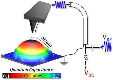
Imaging the quantum capacitance at finite frequency, through RF-EFM, allowed us to gain insight into the effect of H-irradiation on the local MoS2 ML doping level and defect states, and its variation on a submicrometric scale. This technique can be useful to investigate diverse electrostatic phenomena at the mesoscopic scale up to microwave frequencies. Additionally, being nondestructive as a non-contact AFM technique, RF-EFM is robust and can be used for a wide range of applications.
Complete information can be found in ACS Nano.
Two-year post-doc position open
June 2023
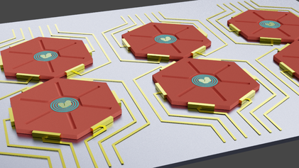 Sketch of the final device comprising an array of strain-tunable cavity-quantum emitter systems.
Creation and study of quantum emitters created in strain-engineered two-dimensional crystals
The post-doc shall be involved in the fabrication and
study of quantum emitters deliberately formed in
two-dimensional crystals under static and dynamical
mechanical deformation. Micro-photoluminescence
and micro-Raman measurements will be performed
in order to assess the strain of the crystals to be
tuned in a controlled manner via deposition and/or
integration in piezoelectric substrates. Second-order
correlation function measurements will be used to
establish the quantum nature of the emitters. These
latter will be eventually integrated in photonics
and/or plasmonic structures in order to enhance the
total and extraction efficiency of the emitter signal.
The position is funded by the QuantERA project EQUAISE (Enabling QUAntum Information by Scalability of Engineered quantum materials).
For further information contact [email protected]
April 2023
A lot of efforts to keep our domes in shape also at low temperature and all we get are ... just single photons generated in spatially controlled sites
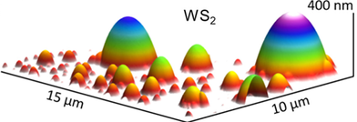 Atomic force microscope image of an ensemble of
molonalayer domes.
Atomic force microscope image of an ensemble of
molonalayer domes.
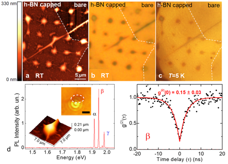
We demonstrated [1] that low-energy hydrogen irradiation of bulk flakes is a reliable and efficient way to form strained, monolayer-thick, H2-filled domes on the surface of the irradiated flakes. Interestingly, strained monolayers can behave as quantum sources [2].
Typically, the H2 liquefaction for temperatures T<32 K causes the disappearance of the domes preventing their use as potential quantum emitters.
We finally succeeded to overcome the dome deflation by depositing thin hexagonal boron nitride flakes on the domes. This leads to the preservation of the dome structure at all temperatures, and finally to the appearance, at 5 K, of intense emission lines originating from localized excitons, which are shown to behave as quantum emitters [3].
The figure below shows the main results of the experiment.
|
a: AFM image of an ordered array of WS2 domes partially capped with a thin (∼10 nm) h-BN flake. The white dashed line marks the border between the h-BN capped area and a bare (i.e. uncapped) area (top-right). b: Optical microscope image of the same area of a, taken at RT. c: Same as b but with the sample at 5 K. The domes in the area capped with h-BN kept their shape, while the bare ones clearly deflated. d: Left, micro-PL spectrum recorded on a single dome showing various emission narrow lines. The lines originate from the edge of the dome, whose AFM image is shown in the bottom inset. The dome belongs to the array shown in panels a, b and c. The narrow emission lines originate from the dome’s edge, as illustrated in the optical microscope image in the top inset showing the dome’s border (white dashed line) and the laser spot, where the lines where excited (black scale bar is 2 micron). Right: Second-order autocorrelation function g(2)(t) recorded on the line beta highlighted in the left panel and exhibiting single photon emission, g(2)(0)<0.5.
|
[1] E. Blundo et al., Nano Letters 22, 1525 (2022); D. Tedeschi, E. Blundo et al., Advanced Materials 31, 1970314 (2019); E. Blundo et al., Physical Review Letters 129, 067402 (2022); E. Blundo et al., Physical Review Letters 127, 046101 (2021)
[2] E. Blundo et al., Applied Physics Reviews 8 021318 (2021); S. Cianci et al., Optical Materials 125, 112087 (2022)
[3] S. Cianci et al., Advanced Optical Materials (2023)
March 2023
Variant Plateau's law in atomically thin crystals: Crystal bubbles behave differently
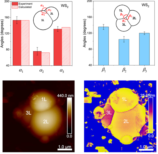 Observation of variant Plateau’s law in bi- and tri-dome systems.
Top left: Histogram of the joint angles in a WS2 bi-bubble systems, extracted
experimentally (solid bars) and analytically (patterned bars). The experimental values for
joint angle are 153.1° ± 8.8°, 75.6° ± 9.8° and 131.2° ± 6.1° for α1, α2 and α3, respectively. Top right: Histogramof the joint angles (βi, i = 1,2,3) in
WS2 tri-bubble systems, extracted experimentally. The experimental values for joint angle are 135.5° ± 6.4°, 104.6° ± 7.1° and 119.9° ± 3.7° for β1, β2 and β3, respectively. Bottom left: AFM image of a WS2 tri-bubble dome
system, consisting of 1 L, 2 L and 3 L domes joint together. Bottom right: Stiffness mapping image of the tri-bubble shown above. The layer-dependent stiffness can be clearly
distinguished.
Observation of variant Plateau’s law in bi- and tri-dome systems.
Top left: Histogram of the joint angles in a WS2 bi-bubble systems, extracted
experimentally (solid bars) and analytically (patterned bars). The experimental values for
joint angle are 153.1° ± 8.8°, 75.6° ± 9.8° and 131.2° ± 6.1° for α1, α2 and α3, respectively. Top right: Histogramof the joint angles (βi, i = 1,2,3) in
WS2 tri-bubble systems, extracted experimentally. The experimental values for joint angle are 135.5° ± 6.4°, 104.6° ± 7.1° and 119.9° ± 3.7° for β1, β2 and β3, respectively. Bottom left: AFM image of a WS2 tri-bubble dome
system, consisting of 1 L, 2 L and 3 L domes joint together. Bottom right: Stiffness mapping image of the tri-bubble shown above. The layer-dependent stiffness can be clearly
distinguished.
Soap bubbles are pretty, coloured, mobile, and fragile. Indeed, soap bubbles are a favourite game for children (and adults…). Nevertheless, these objects have been a model system for fundamental research in equilibrated states involving capillarity and wetting phenomena that have profound implications in living systems and industrial applications [1].
The way bubbles interact and intersect are ruled by the Plateau’s laws dating back to the 19th century [2]. In particular, Joseph Plateau’s fundamental observations of soap bubbles revealed that their borders meet at equal joint angles of 120°.This law has been a prominent physical law in natural sciences. Apart from soap bubbles, Plateau’s law naturally occurs in liquid foams such as beer froth, and in solid foams such as cells, honeycombs, and metallic foams. Whilst some studies have shown that the joint angles in bubbles and foams are not always 120°, the angle deviation is quite small of only a few degrees. Due to the low surface tension of liquids, such as 0.07–0.09 N/m for water and 0.025 N/m for soap bubbles, the capped pressure in liquid bubbles is low and they only exist for short periods of time before bursting.
What should we expect when bubbles occur in solid state systems?
Based on our previous work on transition metal dichalcogenide (TMD) bubbles [3], we successfully created atomically thin TMD bubble networks and observed variant Plateau’s law in such nano-scale solid systems. The results are published in Nature Communications, where it is shown that the variant Plateau’s law is due to thickness dependent stiffness values depending on the bubble layer number, resulting in large effective surface tension differences, which leads to the formation of large joint angle differences of approximately 77° between the largest and smallest angles. This contrasts with the equal joint angles commonly associated with Plateau’s law, demonstrating that this variant is observed due to the 2D TMD bubble network properties. Furthermore, the equivalent surface tension of our TMD bubbles ranges from 2.4 to 3.6N/m, around two orders of magnitude greater than conventional liquid films, enabling the 2D bubbles to sustain high gas pressure and exist in a fundamentally variant nature for several years.
[1] Pierre-Gilles De Gennes , Françoise Brochard-Wyart , and David Quéré, Capillarity and Wetting Phenomena: Drops, Bubbles, Pearls, Waves , (Springer-Verlag, New York, 2004)
[2] J. A. Plateau, Statiqueexpérimentale et théorique des liquids soumis aux seules forces moléculaires. Vol. 2 (Gauthier-Villars,1873)
[3] E. Blundo et al., Nano Letters 22, 1525 (2022); D. Tedeschi, E. Blundo et al., Advanced Materials 31, 1970314 (2019); E. Blundo et al., Physical Review Letters 129, 067402 (2022); E. Blundo et al., Physical Review Letters 127, 046101 (2021)
Boqing Liu, Tanju Yildirim, Tieyu Lü, Elena Blundo, Li Wang, Lixue Jiang, Hongshuai Zou, Lijun Zhang, Huijun Zhao, Zongyou Yin, Fangbao Tian, Antonio Polimeni, and Yuerui Lu, "Variant Plateau’s law in atomically thin transition metal dichalcogenide dome networks", Nature Communications 14, 1050 (2023)
January 2023
Excitons and trions in atomically thin alloys
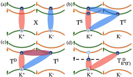
An international collaboration between our group and groups in Poland, France, Czech Republic, and Japan reports on the quantum- and magneto-optical characteristics of a bi-demnsional alloy. The paper has been published in 2D Materials.
October 2022
Invited talk at 2D Materials workshop in Warsaw (24th-26th October 2022)
Antonio Polimeni presented an invited talk on "Bubbles made of two dimensional crystals: magneto- and quantum-optical properties".
The talk can be downloaded here.
October 2022
Our work highlited in the newsletter of the European Magnetic Field Laboratory
|
The European Magnetic Field Laboratory reported on our work on magneto-photoluminescence in highly strained 2D crystals in the EMFL newsletter.
|
|
Septemebr 2022
Elena Blundo is awarded the Nano Letters Seed Grant

The seed grant competition aims to recognize the best research proposal ideas within the scope of Nano Letters from different regions of the world. To highlight the creativity of young researchers, this opportunity is open only to later-stage graduate students (e.g., third year and beyond). The proposed work should be based on the current training and expertise of students and be focused on the next cutting-edge project prior to their graduation. In this way, the seed grant will be grounded in feasibility as well as integrate high-risk, high-reward ideas.
Click here for more information.
Relevant papers:
E. Blundo et al., https://journals.aps.org/prl/abstract/10.1103/PhysRevLett.129.067402
E. Blundo et al., https://pubs.acs.org/doi/full/10.1021/acs.nanolett.1c04197
E. Blundo et al., https://journals.aps.org/prl/abstract/10.1103/PhysRevLett.127.046101
August 2022
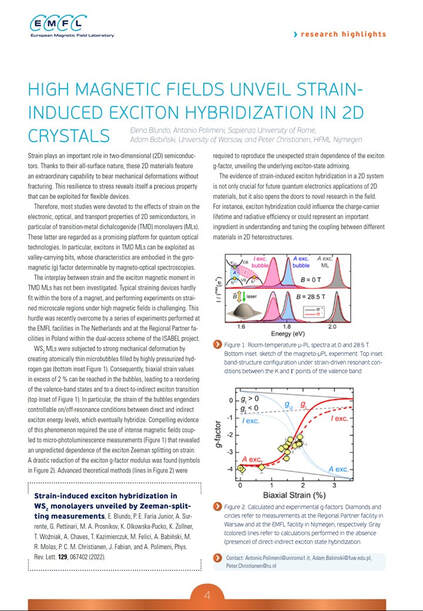
Strained, not stirred... Hybridisation of 2D excitons by stretching
Hybridisation is a ubiquitous phenomenon, playing a crucial role within many seemingly disparate contexts such as chemical-bond formation, light-matter interaction and coupling between discrete states in quantum applications.
Hybridisation phenomena, though, and their potential have not been fully unleashed in two-dimensional (2D) semiconductor crystals.
In a paper published in Physical Review Letters, Elena Blundo and co-authors show that stretching 2D crystals impacts strongly also on the magnetic moments of excitons that can act as the quantum binary information carriers, e.g., in light emitting devices. 2D crystals were subjected to a strong mechanical deformation thanks to the creation of atomically thin microbubbles filled with highly pressurised hydrogen gas. The ensuing strain of the bubbles engenders controllable on/off-resonance conditions between exciton energy levels, which eventually hybridise.
The gathering of compelling evidence of this fundamental, yet subtle phenomenon required the use of intense magnetic fields (up to 28.5 T) at the European Magnetic Field Laboratory (EMFL) facilities in the Netherlands and in Poland. The unprecedented combination of high magnetic and strain fields with optical measurements featuring sub-micron spatial resolution revealed an unpredicted dependence of the exciton Zeeman splitting on strain. Advanced theoretical methods reproduced accurately the unexpected strain dependence of the exciton gyromagnetic factor (the equivalent of Landé factor for atoms), thus unveiling the underlying exciton hybridisation.
The evidence of exciton hybridisation in a 2D system is not only crucial for future quantum electronics applications of 2D materials, but it also opens the doors to new research in the field, wherein, e.g., exciton hybridization could influence the charge-carrier lifetime and radiative efficiency or could represent an important ingredient in understanding the coupling between different materials in 2D heterostructures.
April 2022
Strain unveils mechanical properties of 2D crystals
In collaboration with our colleagues in Salerno and CNR, we peublished a review article on the mechanical, eleastic and adhesive properties of two-dimensional materials in Advanced Materials Interfaces.

March 2022
Review article on 2D crystals
A review paper on the interplay between strain and the electronic properties of two-dimensional materials has been published in Optical Materials.
January 2022
Bubbling hexagonal boron nitride
Paper on hexagonal boron nitride bubbles published in Nano Letters.
|
Hexagonal boron nitride (hBN) is widely used as a protective layer for few-atom-thick crystals and heterostructures (HSs), and it hosts quantum emitters working up to room temperature. In both instances, strain is expected to play an important role, either as an unavoidable presence in the HS fabrication or as a tool to tune the quantum emitter electronic properties. Addressing the role of strain and exploiting its tuning potentiality require the development of efficient methods to control it and of reliable tools to quantify it. Here we present a technique based on hydrogen irradiation to induce the formation of wrinkles and bubbles in hBN, resulting in remarkably high strains of ∼2%. By combining infrared (IR) near-field scanning optical microscopy and micro-Raman measurements with numerical calculations, we characterize the response to strain for both IR-active and Raman-active modes, revealing the potential of the vibrational properties of hBN as highly sensitive strain probes.
|
|
December 2021
QuantERA project funded

|
|
QuantERA is a European Research Programme in the field of Quantum Technologies. Its main objective is to reinforce transnational collaborations between countries in inspiring multidisciplinary quantum research.
The EQUAISE (Enabling QUAntum Information by Scalability of Engineered quantum materials) project focuses on Applied Quantum Science that is aimed at taking known quantum effects and established concepts from quantum science, translating them into technological applications and developing new products.
The project proposes to fabricate arrays of near-ideal single-photon sources realized starting from two-dimensional materials made of transition metal dichalcogenides (TMDs). In the project, mechanics and electrochemistry will be combined to deform and shape two-dimensional membranes made of TMDs at the nanoscale and transform them into site-controlled single photon sources. The sources will be created spatially and spectrally resonant with the electromagnetic field of a microcavity to ensure efficient light extraction. These hybrid structures will be integrated onto micro-machined piezoelectric devices for controlling their emission properties independently by strain engineering. A single chip hosting several non-classical light sources will be fabricated permitting to perform photon processing involving two or more quantum emitters integrated in a single compact device.
July 2021
Tasting adhesion energies in atomically thin sandwiches
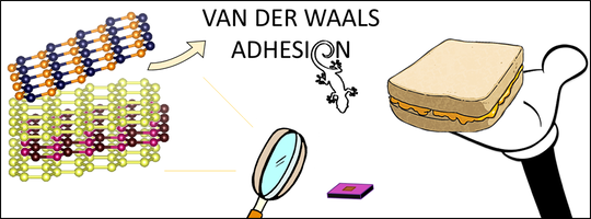
The exfoliation and assembly of van der Waals (vdW) crystals are crucial processes for the fabrication of 2D homo- and hetero-structures. These processes are ruled by the adhesion energy between layers, the determination of which still represents an issue. In a paper published in Physical Review Letters, we present a novel combined experimental and theoretical approach to determine the adhesion energy between 2D crystals. We apply this model to a variety of systems, showing unexpected trends, contrasting those obtained by current DFT-based theoretical methods. Our approach opens new avenues in the flourishing research field on 2D materials and heterostructures and provides insight for the fabrication of vdW-heterostructures.
July 2021

Italian Physical Society prize to Elena Blundo (2nd year PhD student in Physics)
Elena Blundo (PhD in Physics, XXXV cycle) is awarded the “Michele Cantone” prize for Scientific Industriousness. Elena's scientific interests regards the optical, electronic and mechanical properties of two-dimensional materials.
Elena Blundo (PhD in Physics, XXXV cycle) is awarded the “Michele Cantone” prize for Scientific Industriousness. Elena's scientific interests regards the optical, electronic and mechanical properties of two-dimensional materials.
June 2021
Stretchable Flatland
Review article on the great potential of strain to modify the properties of 2D materials published in Applied Physics Reviews
Review article on the great potential of strain to modify the properties of 2D materials published in Applied Physics Reviews
TWO-DIMENSIONAL MATERIALS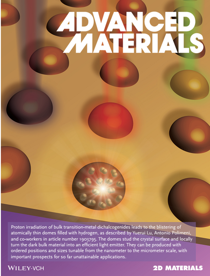
Proton irradiation of bulk transition‐metal dichalcogenides leads to the blistering of atomically thin domes filled with hydrogen,. The domes stud the crystal surface and locally turn the dark bulk material into an efficient light emitter.
Transition metal dichalcogenides, TMDs, of the form MX2 (M=Cr, Mo, or W and X=S, Se, or Te) are layered semiconductors with strong in-plane bonding and weak out-of plane interaction that allows material exfoliation into two-dimensional layers down to a single lattice unit cell. At variance with the zero-gap graphene, TMDs are endowed with a direct band gap providing exciting opportunities in transparent/flexible optoelectronics devices.
We investigate the optical and structural properties of these 2D gapped materials with special emphasis on the effects of hydrogen incorporation. |
Semiconducting Nanowires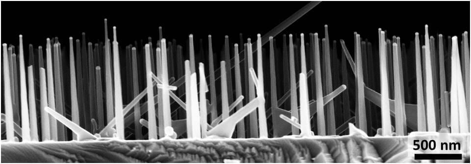 Scanning electron microscopy image of indium phosphide NWs. Notice the gold nanoparticle (serving as catalyst for the NW growth) on top of the nanowires. Scanning electron microscopy image of indium phosphide NWs. Notice the gold nanoparticle (serving as catalyst for the NW growth) on top of the nanowires.
Semiconducting nanowires (NWs) are touted for numerous applications in electronics, optoelectronics, energy, and health sciences, and have displayed rich and unique behaviors in their growth and physical properties.
In the past few years, we have addressed several topical issues related to the electronic and structural properties of these fascinating nanostructures employing state-of-the-art optical techniques. In particular, the combined use of very intense magnetic fields (up to 30 T) with emission spectroscopy allowed for the understanding of transport and spin properties of III-V NWs. |
Nanostructures and Photonics
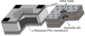
Sketch of a photonic crystal cavity embedding a GaAsN quantum dot obtained by spatially selective H irradiation.
The investigation of light-matter coupling phenomena has been made available by the development of techniques allowing for the integration of nm-sized emitters with optical cavities of (sub-) micrometric dimensions, such as photonic crystal microcavities (PhCs).
In this context, our group developed a novel method, whereby spatially selective irradiation of III-V alloys with hydrogen permits the creation of site- and energy-controlled quantum dots within a PhC. The emission properties of the dots are determined on a sub-micron scale length via advanced microscopy techniques. |
hydrogen in novel materials
|
Hydrogen is the smallest atom and one of the most chemically reactive elements. These H characteristics account for its high diffusivity and reactivity in semiconductors, where it can sizeably affect the electrical, magnetic and electronic properties of the material. H presence in (and subsequent removal from) p-doped GaN enabled the discovery of white LEDs. H was also recently found to turn highly conductive graphene into an insulator. The capability of H to wipe out energy levels of shallow impurities and defects from the forbidden energy gap has been largely investigated and exploited.
In recent years, our group employed low-energy H irradiation in a large variety of semiconductor materials, nanostructures, and light emitting devices. Follow the link to know more. |
|