HYDROGEN IN NOVEL MATERIALS
INTRODUCTION
Hydrogen is an impurity ubiquitous in most phases of growth and processing of semiconductor materials and, hence, in the mass-production of electronic devices. The importance of H-induced effects in semiconductors stems from the high chemical reactivity and diffusivity of this element. Indeed, H tends to bind to dangling bonds associated to point and extended defects and thus cleans up the band gap from the energy levels related to those defects. This process, usually referred to as defect passivation, leads to a large modification of conductivity in most semiconductors and removes often the detrimental consequences caused by crystal imperfections. In particular, the formation of complexes made of H atoms and impurities has been observed in a vast number of elemental, compound, and alloyed semiconductors. H also turns conductivity from p-type into n-type in diamond, neutralizes the native p-type conductivity in Ga(AsBi) alloys, and transforms graphene from a highly conductive semimetal into an insulator.
Interestingly, hydrogen itself may act as a dopant in narrow gap semiconductors and in III-nitrides, such as GaN and AlN. In the latter case, H promotes the incorporation of p-type impurities (e.g., Mg) and, once H is thermally removed, allows for p-type doping of GaN and related materials. This effect represented the breakthrough that led to invention of the first blue LED (2014 Nobel prize) and then to the mass production of white LEDs.
OUR RESEARCH (thesis available)
Our group has a strong background on the study of the effects of H incorporation on the electronic properties of semiconductor materials and nanostructures.
Hydrogen irradiation of semiconducting samples can be performed by means of a low-energy (1-500 eV) Kaufman source, operating at temperatures ranging from room temperature to 600 °C. The figure below sketches the hydrogenation apparatus we employ to incorporate H into solids.
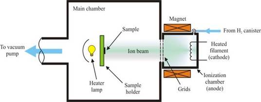
Detail of the Kaufman source employed for hydrogen irradiaton. The electrons ejected dissociate H molecules and the grid system focus H+ ions on the sample suitable heated and electrically grounded.
Among the results we obtained over the years, we mention the increase in the emission efficiency of InAs self-assembled quantum dots, a system widely investigated nowadays as efficient single photon sources. H irradiation was found indeed to improve the photoluminescence yield by nearly a factor 1000 (see paper in Applied Physics Letters).
We also found (see reference in Applied Physics Letters) that H neutralizes the native p-type conductivity in Ga(AsBi) alloys, a material system of interest for photovoltaics and telecommunications.
Interestingly, H irradiation can modify the performances of optoelectronic devices. We reported in Applied Physics Letters the fabrication of a micrometer-size movable light emitting area in a GaAs/AlAs quantum well (QW) resonant tunneling p-i-n diode. We showed that after hydrogenation the position of the QW electroluminescence (EL) area can be spatially shifted by the applied voltage and that the bias condition for the resonant injection of electrons and holes into the bound states of the QW changes across the mesa. In turn, this can lead to the simultaneous resonant tunneling injection of electrons and holes into the QW at specific positions of the diode, thus resulting in a tenfold increase of the local EL intensity, as shown in the figure below.
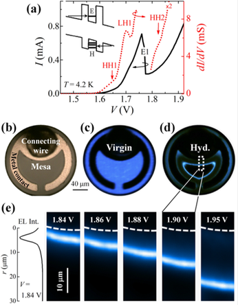
A movable light emitting area by post-growth hydrogenation of a RT-LED. (a) Current-voltage I(V) characteristics of a virgin 200 μm diameter mesa RT-LED at T = 4.2 K. This is dominated by a strong resonance due to tunneling of electrons into the E1 QW subband and by much weaker resonances—observed in the conductance dI/dV—due to tunneling of holes into the HH1, LH1, and HH2 QW subbands; see inset for a sketch of the carrier injection into the QW. (b) Optical image of a 200 μm diameter mesa RT-LED. (c) and (d) Digital camera images of the EL emission intensity (at T = 9 K and V = 1.9 V) before [Virgin, (c)] and after [Hyd., (d)] post-growth hydrogen incorporation. The images were acquired with an 800 nm short-pass filter to remove the contribution from the GaAs spacer and contact layers. (e) Normalized EL maps for increasing values of the applied voltage, as obtained by plotting the EL intensity (atT = 9 K) around the QW emission energy (E = 1.63 eV). The dashed lines in the EL maps indicate the metal contact edge. The EL spatial profile is also shown for V = 1.84 V.
The ability to spatially localize and move on a micrometer scale the emitting region in a LED is relevant for several applications including Lab-On-a-Chip experiments, bio-imaging, high-resolution micro-displays, optoelectronic integrated circuits, etc. As several innovative device concepts in emerging nanotechnologies exploit the quantum tunneling of charge carriers into a quantum state, our approach could be extended to other applications of resonant tunneling that span from optoelectronic integrated circuits to electrically pumped quantum devices.
Hydrogen can be also employed as a probe to address the microscopic mechanisms that regulate carriers injection into nanostructures. A recent example published in Nano Letters is provided by the discovery of the laser level scheme of Ge quantum dots encapsulated in Si. The next picture shows a Ge dot in which a a split-[110] self-interstitial surrounded by a distorted crystal lattice forms and allows direct transitions of electrons localized at the split-interstitial with holes confined in the Ge QD.
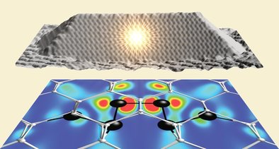
Top: sketch of a Ge quantum dot. Bottom: Electronic orbital electron density
cross sections in the plane containing the split interstitial
Another remarkable effect of hydrogen on the electronic properties of a low-gap III-nitrides: InN and InGaN. It is well known that substitution of constituent atoms and/or changes of crystal structure modify the fundamental properties of a semiconductor. We reported in Advanced Functional Materials that such a tailoring can also be realized thanks to a novel hydrogen effect. Four hydrogen atoms (see next figure) can screen the effect the crystal potential has on a constituent cation, thus generating a solitary cation: an effectively isolated impurity, so chemically different from the unscreened constituent cations that it strongly perturbs the electronic properties of the material by increasing its fundamental band-gap energy. Such a hydrogen-induced screening effect is removed by thermal treatments, thus permitting reversible modifications of both the “crystal chemistry” and material's properties.
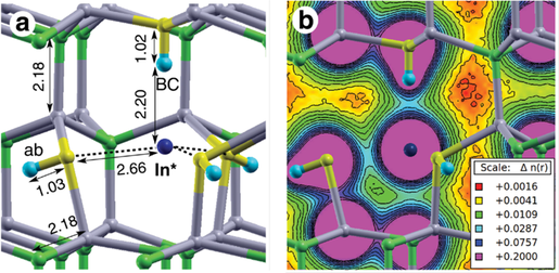
HBC–3Hab complex and In* solitary cation. a) Geometry of the HBC–3Hab complex in InN. Light-blue: H, yellow: N, dark-blue: In* solitary cation. In and N atoms of the bulk InN are represented by grey and green spheres, respectively. Bond distances are given in angstroms.
b) Isoelectronic contours of the total charge density taken around the defect. Color-code for the isoelectronic contour is displayed in the inset; values are in e Bohr−3 units.
This phenomenon, observed in InN and other topical nitrides, should permit the development of a new class of materials as well as the fabrication of photonic devices and optical integrated circuits with distinct, tailor-made regions emitting or absorbing light, all integrated onto a monolithic semiconductor structure.
