nanostructures and photonics
INTRODUCTION
In the last twenty years, the investigation of light-matter coupling phenomena has pushed its boundaries beyond the fundamental limit represented by the wavelength of light (about 1 μm for visible/near infrared light). This intriguing possibility was made available by the development of techniques allowing for the integration of nm-sized emitters -mainly quantum dots (QDs), but also quantum wires (QWRs) and radiative defects (e.g., NV centers in diamond)- with optical cavities of (sub-) micrometric dimensions, such as micropillars and photonic crystal (PhC) microcavities. These nm-sized emitters are endowed with the capability of emitting single photons, a prerequisite for quantum optics protocols. Several examples of light sources that exhibit a non-classical behaviour exist in nature, as shown in the figure below.
In the last twenty years, the investigation of light-matter coupling phenomena has pushed its boundaries beyond the fundamental limit represented by the wavelength of light (about 1 μm for visible/near infrared light). This intriguing possibility was made available by the development of techniques allowing for the integration of nm-sized emitters -mainly quantum dots (QDs), but also quantum wires (QWRs) and radiative defects (e.g., NV centers in diamond)- with optical cavities of (sub-) micrometric dimensions, such as micropillars and photonic crystal (PhC) microcavities. These nm-sized emitters are endowed with the capability of emitting single photons, a prerequisite for quantum optics protocols. Several examples of light sources that exhibit a non-classical behaviour exist in nature, as shown in the figure below.
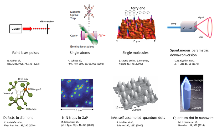
Examples of single photon sources. The bottom row refers to semiconductor-based sources that can be integrated into optoelectronic devices.
However, not all single photon sources can be integrated or confined in small spatial regions such as optoelectronic devices and PhC microcavities. To this respect, single photon sources made of semiconductor materials are unique.
PhC microcavities have emerged as ideal candidates for controlling the emission of photons emitted by manipulating the electromagnetic field distribution in the surroundings of a light emitter. Indeed, photonic crystals are dielectric (or semiconductor) materials in which the dielectric function is periodically modulated in 1, 2, or 3 dimensions. A periodically patterned slab can block propagation of certain frequencies in all directions. The range of frequencies for which propagation is prohibited is called the photonic band gap. However, if the photonic crystal symmetry is broken, for instance by introducing a defect altering the crystal periodicity, states form within the photonic band gap. These states form modes which are laterally confined by the surrounding photonic crystal and the associated electromagnetic field is strongly localized around the defect (see next figure).
PhC microcavities have emerged as ideal candidates for controlling the emission of photons emitted by manipulating the electromagnetic field distribution in the surroundings of a light emitter. Indeed, photonic crystals are dielectric (or semiconductor) materials in which the dielectric function is periodically modulated in 1, 2, or 3 dimensions. A periodically patterned slab can block propagation of certain frequencies in all directions. The range of frequencies for which propagation is prohibited is called the photonic band gap. However, if the photonic crystal symmetry is broken, for instance by introducing a defect altering the crystal periodicity, states form within the photonic band gap. These states form modes which are laterally confined by the surrounding photonic crystal and the associated electromagnetic field is strongly localized around the defect (see next figure).
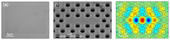
(a) Scanning electron microscopy image of a SiC (silicon carbide) PhC cavity containing a line defect in its center. (b) Enlarged view of the defect region. (c) Distribution of the electromagnetic field localized around the line defect.
Among the many advantages of PhC cavities, the most important are probably represented by the relative ease of fabrication and by the possibility of achieving high quality (Q) factors -i.e., low radiative losses, long intracavity photon lifetimes, narrow spectral linewidths- and small modal volumes. This has recently allowed for the observation of strong-coupling phenomena in a single QD-PhC cavity integrated system, and it carries great promise for the realization of numerous applications. In spite of these accomplishments, however, the field of nanophotonics is still in its infancy. The departure from this pioneering phase will require the emergence of novel methods for the design and fabrication of photonic devices, offering the possibility to control both the electromagnetic field distribution of the optical modes confined in the photonic structure and the spatial/spectral position of the integrated light emitters.
OUR RESEARCH (thesis available)
Our approach to the integration of single photon sources within PhC cavities combine materials science, state-of-the-art lithographic techniques, defect engineering and advanced tools for the modeling and the design of photonic devices. One of the cornerstones of our research is represented by a novel method for the fabrication of site-controlled nano-emitters -based on the hydrogen-induced passivation of N atoms in dilute-nitride semiconductors- that was pioneered by our group.
A novel route to site-controlled quantum dots
In dilute nitrides (e.g., GaAsN, InGaAsN, GaPN), the formation of stable N-2H-H complexes (see next figure) following H irradiation wipes out the effects of nitrogen on the optical (i.e., refractive index), structural and electronic properties of the material. In particular, H binding to N atoms in GaPN leads to an increase in the band gap energy of the N-containing material (red emitting sample in the figure below) up to its GaP value (green emitting sample in the figure below).
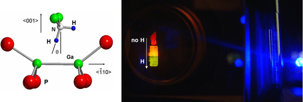
Left. N-2H-N complex responsible for the electronic passivation of N in GaPN, and other dilute nitride materials, such as GaAsN and InGaAsN. Right. Picture of three GaPN irradiated with different H doses showing a change in the emitted light color corresponding to an increase of the crystal band gap energy. The blue light on the right is the exciting laser.
Importantly, by allowing H incorporation only in selected regions of the sample (for example by deposition of H-opaque metallic masks prior to hydrogenation), it is possible to attain a spatially controlled modulation of the band gap energy in the growth plane. As discussed in this work published in Advanced Functional Materials, this technique -henceforth referred to as In-plane Band Gap Engineering (BGE)- can eventually be employed to tailor the carrier-confining potential down to the nm level, resulting in the fabrication of site-controlled, dilute nitride-based QDs. BGE steps and final results are summarised in the next figure. Details can be found in M. Felici et al. (Advanced Materials), R. Trotta et al. (Advanced Functional Materials), and S. Birindelli et al. (Nano Letters).
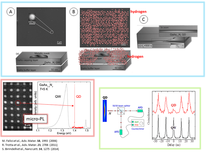
Blue box. Band gap engineering outline. (a) H-opaque mask deposition. The mask is made of 100 nm circles that impede H diffusion beneath them. The sample consists of a single GaAsN quantum well, QW, sandwiched between GaAs barriers. (b) Exposure of patterned sample to H that diffuses everywhere but a nm-sized region beneath the mask. (c) Eventually, a GaAsN quantum dot, QD, forms in a GaAs barrier.
Red box. Micro-PL image showing the perfect uniformity and 100% yield of the dot fabrication process. The emission spectrum from a single QD (red-circled region) shows the typical atomic-like spectrum of a zero-dimensional nanostructure (at variance with the broad emission from the starting QW).
Green box. Photon correlation measurements showing that the QD exhibits a non-classical behaviour.
Embedding a QD in a photonic crystal cavity
The inherently precise control over the position of the nanostructures fabricated with this method renders them naturally suited for the integration with PhC microcavities. The nano-emitters fabricated by In-plane BGE will be integrated with PhC microcavities of new conception, developed by making use of the semi-analytic method for PhC cavity design introduced by M. Felici et al. in Physical Review B. Through the definition of a direct relationship between the target electromagnetic field distribution and the dielectric constant of the cavity supporting it, this innovative method eliminates the need for the cumbersome, computationally demanding trial-and-error procedures that currently hinder further developments in the field of PhC cavity design.
Form the experimental point of view, we recently succeeded in coupling a GaAsN QD with the cavity mode of PhC. In the next figure, the method employed is schematically shown. More complicated geometries and QDs emitting at 1310 nm are under development under the umbrella of an Innovative Training Network project named Postgraduate Research on Dilute Metamorphic Nanostructures and Metamaterials in Semiconductor Photonics (PROMIS) funded by the EU within the Horizon 2020 framework.
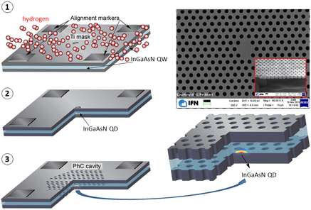
Left. Main steps leading to the formation of an InGaAsN QD in a PhC cavity.
(1) Hydrogenation of a lithographically patterned InGaAsN quantum well. (2) Formation of an InGaAsN quantum dot. (3) Subsequent creation of a PhC cavity around the dot exploiting the alignment markers.
Right. Zoom in of the dot located in the defect region of the PhC cavity, where the electromagnetic field density is maximum. On top of the zoomed figure, scanning electron microscopy image of the actual device (courtesy of Dr. G. Pettinari at IFN, CNR Rome).
