
Thesis available
Master and PhD thesis are available in the different topics investigated in our group.
In all cases, the student will be involved in optical spectroscopy measurements and their analysis. When necessary, modifications and implementations of the available set-ups will be made. The student will work in collaboration with the material growers and other researchers investigating the morphological and structural properties.
In all cases, the student will be involved in optical spectroscopy measurements and their analysis. When necessary, modifications and implementations of the available set-ups will be made. The student will work in collaboration with the material growers and other researchers investigating the morphological and structural properties.
Nanowires
- Exploring the Aharonov-Bohm effect in quantum well tubes
Enormous progresses have been made in the growth of semiconductor nanowires (NWs). In particular, lateral overgrowth on NW surface permits the synthesis of core-shell NWs in which the wire chemical composition varies radially; see figure.
In this thesis, the aim is the study of the electronic properties of GaAs quantum well tubes (QWTs) embedded in InP NWs by photoluminescence (PL) under magnetic field, B.
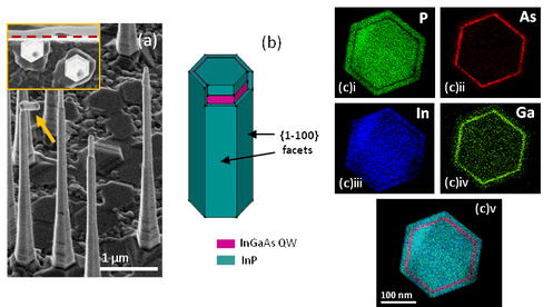
(a) Scanning electron microscopy image of a quantum well tube in a NW. (b) Compositinal schematic of the nanostructure. (c) Energy dispersive x-ray (EDX) compositional maps; i.-iv. elemental EDX maps of P, As, In and Ga, respectively. v. Over lay of all elemental maps shown.
As a matter of fact, the circular symmetry of the tube prompts the opportunity of studying optically the Aharonov-Bohm (AB) effect that is a quantum mechanical phenomenon inducing a phase shift on the wave function of a charged particle as it orbits a magnetic flux in a closed trajectory.
Measurements are planned at the European Magnetic Field Laboratory (EMFL) facility in Nijmegen on July 2017. A through study of the nanostructures will be performed prior to magnetic field measurements.
Measurements are planned at the European Magnetic Field Laboratory (EMFL) facility in Nijmegen on July 2017. A through study of the nanostructures will be performed prior to magnetic field measurements.
- Study of the carrier temperature gradient in kinked nanowires
Kinked nanowires are peculiar nanostructures in which the crystal phase changes abruptly from zincblende to wurtzite. Also, the NW diameter decreases from 120 to 70 nm on changing phase. Most importantly, this diameter variation may lead to a drastic change in the photogenerated carrier temperature, which is not in equilibrium with the lattice temperature, as we demonstrated in this work (see also figure).
Kinked nanowires are peculiar nanostructures in which the crystal phase changes abruptly from zincblende to wurtzite. Also, the NW diameter decreases from 120 to 70 nm on changing phase. Most importantly, this diameter variation may lead to a drastic change in the photogenerated carrier temperature, which is not in equilibrium with the lattice temperature, as we demonstrated in this work (see also figure).
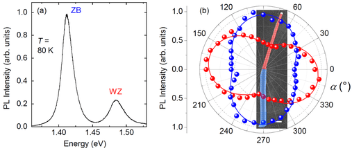
Left. Photoluminescence spectrum of a kinked Nw showing emission from the ZB and WZ section. Right. Polar plot of the PL intensity showing that WZ and ZB emission is polarized mainly orthogonal and parallel to the NW axis.
In this thesis, it will be investigated this peculiar phenomenon under the action of an externally applied bias in order to explore the possibility of observing an electron Seedback effect. The sketch of the device is shown below.
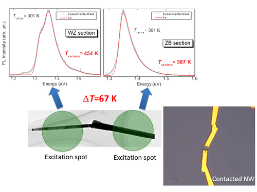
Top. PL spectra of the WZ and ZB section of a kinked NW. Below. Transmission electron microscopy image of a kinked NW. A contacted NW is also shown by scanning electron microscopy.
Transition metal dichalcogenides
Transition metal dichalcogenides, TMDs, of the form MX2 (M=Cr, Mo, or W and X=S, Se, or Te) are layered semiconductors with strong in-plane bonding and weak out-of plane interaction that allows material exfoliation into two-dimensional layers with a few or even a single lattice unit cell. This latter configuration determines a transition from indirect to direct band gap providing exciting opportunities in transparent/flexible optoelectronics devices.
Transition metal dichalcogenides, TMDs, of the form MX2 (M=Cr, Mo, or W and X=S, Se, or Te) are layered semiconductors with strong in-plane bonding and weak out-of plane interaction that allows material exfoliation into two-dimensional layers with a few or even a single lattice unit cell. This latter configuration determines a transition from indirect to direct band gap providing exciting opportunities in transparent/flexible optoelectronics devices.
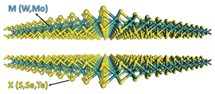
Sketch of the layered structure of transition metal dichalcogenides of the MX2 form.
This thesis will focus on the effects of light atom (H and He) irradiation on the electronic and vibrational properties of TMDs studied by micro-photoluminescence and micro-Raman spectroscopies. Samples consist of 10 micron-sized flakes deposited on SiO2. Each flake contains regions with a number of layers n ranging from n=1 to n>4 (bulk limit). A low-energy (1-100 eV) Kaufman source will be employed to controllably alter the pristine bonds of single- and few-layer samples by hydrogen and helium. Specifically, the high chemical reactivity of H will be exploited to break/modify the strong intra-layer bonds between the metal and the chalcogen atoms, thus leading to drastic, yet tunable, changes in the material physical properties. Also, H atoms are expected to saturate dangling bonds at the flake boundaries thus determining an increase in the efficiency of the radiative recombination process of carriers. This has been indeed observed by us recently, as shown in the figure below, and it will be investigated systematically.
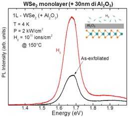
PL spectra of WS2 sigle layer samples prior (as-exfoliated) and after irradiation with atomic hydrogen. Notice the intensity increase after hydrogenation.
Another very recent puzzling topic regards the observation of H-induced blistering of TMDs in the bulk form. Indeed, micron- and submicron-sized bubbles form following hydrogen irradiation. Strikingly, those bubbles emit light very efficiently in contrast with the surronding bulk material thus paving the way to the engineering of spatially controlled light emitting sources. The bubbles are likely filleb by molecular hydrogen ensuing a hydrogen evolution reaction beneath the flake surface. The next figure shows a comparison between AFM and micro-PL mappings of the same region of a WS2 flake.
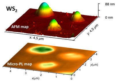
Top. Atomic force microscopy image of hydrogen gas traped in a WS2 cage having one monolayer skin thickness. Bottom. Micro-PL mapping of the same region.
InGaAsN quantum dots embedded in photonic crystal cavities
The capability of atomic hydrogen to passivate N in III-N-V semiconductors (e.g., GaAsN, InGaAsN and GaPN) provides us with an exceptional tool to fine tune on a nanometer scale the band gap (as well as the refractive index and the lattice constant) of these materials featuring interest for photovoltaics and telecommunications.
In this thesis, it will be explored the possibility to deterministically place an InGaAsN quantum dot emitting at 1310 nm in a photonic crystal cavity following the protocol outlined in the next figure.
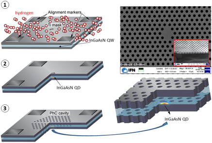
Left. Main steps leading to the formation of an InGaAsN QD in a PhC cavity.
(1) Hydrogenation of a lithographically patterned InGaAsN quantum well. (2) Formation of an InGaAsN quantum dot. (3) Subsequent creation of a PhC cavity around the dot exploiting the alignment markers.
Right. Zoom in of the dot located in the defect region of the PhC cavity, where the electromagnetic field density is maximum. On top of the zoomed figure, scanning electron microscopy image of the actual device (courtesy of Dr. G. Pettinari at IFN, CNR Rome).
