semiconducting Nanowires
INTRODUCTION
Nanowires (NWs) are filamentary crystals with a diameter of the order of a few nanometers. Their increasing importance in both science and engineering is a consequence of the great number of novel experiments and applications they enable. A typical ‘bottom-up’ nanowire synthesis process involves Vapor–Liquid–Solid (VLS) or vapor–solid growth mechanisms in which nanoparticles are used as catalysts to continuously feed the one-dimensional (1-D) material growth [1], as shown in the next picture.
Nanowires (NWs) are filamentary crystals with a diameter of the order of a few nanometers. Their increasing importance in both science and engineering is a consequence of the great number of novel experiments and applications they enable. A typical ‘bottom-up’ nanowire synthesis process involves Vapor–Liquid–Solid (VLS) or vapor–solid growth mechanisms in which nanoparticles are used as catalysts to continuously feed the one-dimensional (1-D) material growth [1], as shown in the next picture.
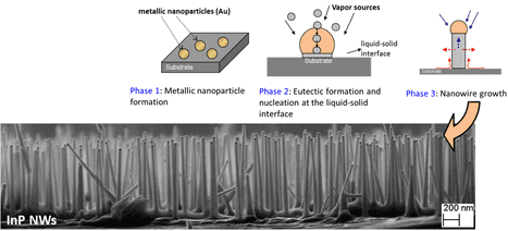
Top. Sketch of the vapour-liquid-solid (VLS) mechanism leading to the formation of NWs.
Bottom. Scanning electron microscopy images of InP NWs grown at the Australian National University (lead Prof. Jagadish). The image was recorded by F. Mura at CNIS (Centro di ricerca per le Nanotecnologie applicate all'Ingegneria, Sapienza università di Roma).
NWs can be also grown by the Selective Area Epitaxy (SAE) method [2], in which the substrate is masked with a patterned SiO2 layer and growth conditions are appropriately selected to confine the epitaxial growth inside the holes, see following figure. Being based on a patterned substrate, SAE has emerged as the most suitable method to provide regular and homogeneous arrays of NWs with perfect vertical yield.
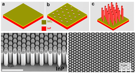
Top. Steps of NW growth by SAE. a: SiO2 deposition; b: lithographic patterning; c: epitaxial NW growth. Bottom. Scanning electron micrsopy side- (left) and top- view (right) of an ensemble of perfectly ordered InP NWs. Growth and images were performed at the Australian National University.
The beauty of both approaches lies in the ability to grow a wide range of nanowire materials, including group IV, III–V and II–VI core/shell, superlattice and branched structures, while simultaneously allowing precise control of the nanowire composition, morphology and electrical properties through fine tuning of growth parameters that enhance or suppress the axial and radial growth processes [3]. It has been shown that the reduced diameter of nanowires allows the combination of lattice-mismatched materials when they are fabricated in the nanowire form. For instance, the next picture shows core-shell NWs in which the composition is veried radially leading to the formation of a tubular quantum well (QW).
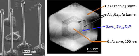
Left. Scanning electron microspy images of core-shell NWs grown by the VLS method. Right. Transmission electron microscopy (TEM) image of one of the NWs shown in the left panel. Samples were grown and images were recorded at the Australian National University.
Nowadays, after several decades of effort, semiconducting nanowire research has streamlined into several frontiers, namely nanoelectronics, nanophotonics, nanoelectronic-bio interfaces, optoelectronics and energy harvesting/conversion and storage (see below). Though, innovative ideas or device concepts are still in great need for next generation smart and integrated nanoelectronic and nanophotonic devices for biological scaffolds.
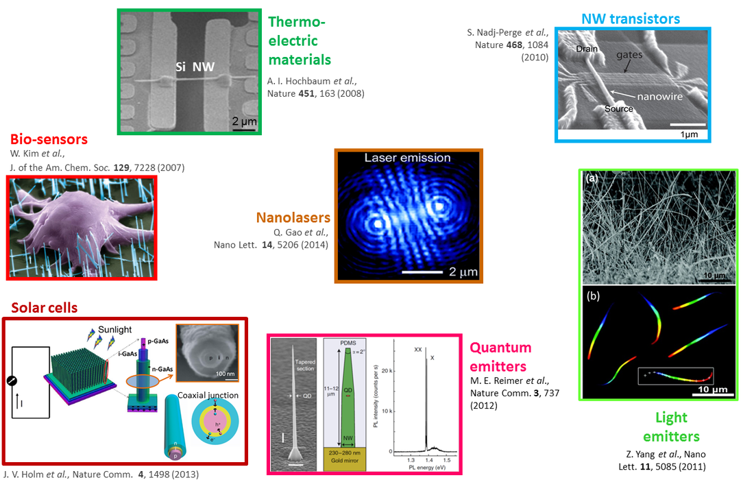
Bird-of-eye view of NW applications that exploit the highly anisotropic morphology of these nanostructures.
OUR RESEARCH (thesis available)
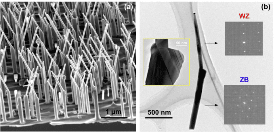
One of the most exciting properties of NWs is their capability to grow with different crystal phases, known as polytypism [4], which has provided a platform for fundamental studies and technological applications.
In fact, the high surface-to-volume ratio of NWs leads to the formation of crystal phases not attainable in the same semiconductors at ambient conditions. Specifically for non-nitride III-V compounds (such as, GaAs, InP, InAs, GaSb, etc.), the wurtzite lattice can be often found at variance with bulk and thin film crystals, where only the zincblende phase is observed. Notably, the WZ phase usually features a band gap energy greater than its ZB counterpart. However, this complication has been soon turned into a potential feature to be exploited, e.g. in NW homostructures in which ZB and WZ phases alternate controllably and thus band gap engineering is achieved.
Indeed, thanks to the enormous progress achieved in the growth of III-V NWs, it is possible to controllably switch between the WZ and ZB lattice thus allowing for the synthesis of NW homostructures (see next figure), where it is the alternation of the crystal phase instead of the composition that provides the band gap discontinuities. This approach has led to the fabrication of 1D superlattices, quantum wells, and nanodots embedded in NWs featuring minimal strain and null composition inhomogeneity with great prospects in several applicative fields. At the same time, these novel low-dimensional structures have prompted the necessity of a full understanding of the basic electronic properties of the WZ lattice of non-nitride III-V compounds (e.g., InP, InAs, and GaAs).
|
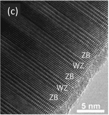
(a) Scanning electron microscopy image of an ensemble of kinked InP NWs made of two different crystal phases, as shown in (b) by transmission electron microsocpy. (c) shows that the alternation of WZ and ZB can be controlled perfectly. |
Mind the gap: The case of GaAs and InAs wurtzite NWs
ZB GaAs, along with Si, is the most investigated semiconductor, but in the case of WZ GaAs NWs, even the band gap energy value is still debated. Likewise, InAs has been widely studied because of its enhanced transport properties. However, most of the electronic properties WZ InAs (found uniquely in the NW form) are unknown.
Our group determined the band gap energy of both these technologically relevant NW systems by various opical techniques (PL, PLE, polarization-dependent PL). The results are summarized in the next figure showing that the exciton band gap energy at T=10 K of WZ GaAs (see reference in Physical Review B) and InAs (see reference in Nano Letters) are 1.523 eV (1.515 eV in ZB) and 0.477 eV (0.418 eV in ZB), respectively.
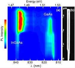
(a) Micro-PL mapping of a single WZ InGaAs/GaAs core-shell NW showing the emission of the exciton band gap at 1.523 eV. (b). Scanning electron microscopy of the same NW (click on figure for details).
|
Letf. PL (right axis) and PL polarization degree (left axis) of WZ InAs NWs. The ZB emission is due to the substrate. The NW emission is clearly polarized orthogonal to the wire axis, as expected for WZ crystals. Right. Polar plot of the PL intensity confirming the WZ phase of the NWs (click on figure for details).
|
Band structure of WZ InP NWs
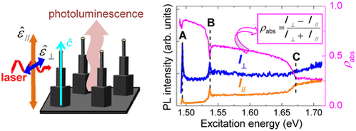 Left. Sketch of the experimental configuration for polarization-dependent PLE. Right. PLE spectra (left axis) under excitation parallel and orthogonal to the NW c axis. Notice the different polarization-related selection rules of the A, B, and C WZ critical points. Polarization degree (right axis) of the NW absorption. Click on figure for details.
We performed a through investigation of the WZ crystal structure in high-quality InP NWs. We determined with high precision the energy and the selection rules of the critical points of the InP WZ band structure. Polarization-dependent PLE measurements were employed to this end allowing us to draw a complete picture of the absorption mechanisms occurring in WZ InP NWs that is useful in the design of optoelectronic devices, such as solar cells and photodetectors.
Furthermore, we unveiled subtle effects related to the enhancement in the dielectric mismatch effect between the NWs and the enviroment originating from the Coulomb interaction between electron and hole. Refer to this article published in Nano Letters.
Furthermore, we unveiled subtle effects related to the enhancement in the dielectric mismatch effect between the NWs and the enviroment originating from the Coulomb interaction between electron and hole. Refer to this article published in Nano Letters.
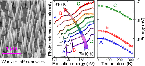
Left. Scanning electron microscopy image of an ensemble of InP WZ NWs. Center. Temeprature-dependent PLE measurements. A, B, and C indicate the loest-energy critical points of the WZ InP band structure and temperature dependence of their enrgy (right). Click on figure for details.
|
Further precious information on the band structure of WZ InP NWs were gathered by temperature-dependent PLE measurements that are shown in the figure on the left. These studies demonstrated a general feature of the thermal properties of WZ materials that holds regardless of the bond polarity and energy gap of the crystal. Furthermore, we found that a negligible role is played by the WZ/ZB differences in determining the deformation potentials and the extent of the electron–phonon interaction that is a direct consequence of the similar nearest neighbor arrangement in the two lattices (see the ACS Nano paper).
|
Light absorption processes and photo-excited carrier relaxation phenomena in NWs
|
Core-shell NWs are usually employed to reduce the surface carrier recombination in bare NWs. The surface is usually passivated by wrapping the NW core with a thin shell. However, light absorption occurring in the shell may affect the carrier relaxation toward the core, thus reducing the cell efficiency.
We investigated this phenomenon in InGaAs-GaAs core-shell NWs. In particular, we showed that photogenerated carrier relaxation toward the InGaAs core is siazably influenced by carrier recombination in the shell as shown in the figure on the left. In fact, anti-resonances are observed in the PLE spectrum relative to absorption in the InGaAs core at energies matching the DOS of the GaAs shell (see paper in Applied Physics letters for details). |
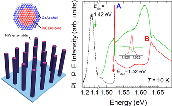
PL and PLE spectra of an ensemble of InGaAs-GaAs core-shell NWs. Depending on the detection energy Edet a resonance (Edet=shell band gap energy) or an antiresonance (Edet=core band gap energy) is observed (click on figure for details).
|
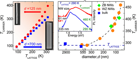 Left. Carrier temperature vs lattice temperature in NWs with different diameter d. Clearly, out-of-equilibrium conditions establish in the small NW. Right. Dependence of the carrier temperature on NW diameter. The inset shows two typical PL spectra under cw excitation for NWs with different diameter (click on figure to know more).
Another interesting phenomenon we discovered in NWs is the existence of long-lived hot carriers and published in Nano Letters, namely laser-generated clouds of electrons and holes, whose temperature is much higher than that of the NW lattice where carriers are confined. It has to be stressed that, while hot carriers are usually observed few ps after a laser pulse, here we observe for the first time hot carriers under steady state excitation. In particular, we found that the thermal mismatch between carriers and lattice increases dramatically with decreasing the NW diameter, as shown in the next figure. Moreover, these findings is a general feature of anowires, being independent on composition, crystal phase, and morphology.
Addressing the transport and spin properties of wurtzite nanowires
by photoluminescence under high magnetic field
by photoluminescence under high magnetic field
The use of external perturbations in a PL experiment permits to deduce valuable information about the electronic states at the optical band gap. In particular, magnetic fields, B, affect position and lift degeneracy of energy levels involved in spectroscopically observed transitions. The extent of the modifications induced by a magnetic field on the eigenstates of charge carriers in a semiconductor nanostructure depends on several factors. One of the most relevant is the relative strength of the perturbation provided by the field, usually gauged by the cyclotron energy, with respect to the Coulomb interaction between electrons and holes (whose extent varies with the nanostructure size/shape). The quantitative analysis of the interplay between the Lorentz and Coulomb forces provides extremely important information on several fundamental quantities, such as the charge carrier effective mass, the gyromagnetic factor of electrons and holes, their wavefunction extent/shape, etc.
It is common practice to employ the bulk values of these quantities for estimating the electronic and optical properties of nanostructures and quantum heterostructures. However, this approach breaks down in most NWs, which grow very often in the WZ phase crystal phase not existing in the bulk form, where instead ZB is ubiquitous. As a consequence, even some basic band structure properties are not very well known in WZ NWs.
We used high magnetic fields (B=30 T) at the European Magnetic Field Laboratory (EMFL) in Nijmegen to address the fundamental properties of InP WZ NWs, in particular the effective mass of electrons and holes and the exciton gyromagnetic factor. The inherently anisotropic properties of the WZ lattice were investigating by steering the magnetic field along different directions with respect to the NW axis. The following pictures depicts the main results obtained on InP WZ NWs grown by VLS and SAE and exhibiting different morphologies, but giving identical results.
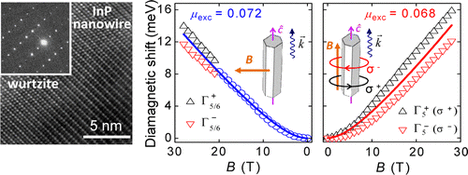
The figure on the right shows the diamagnetic shift of excitons in WZ InP NWs grown by VLS, whose transmission electron microscopy image is shown on the left panel. As depicted in the insets of the right figure, two different field configurations were employed leading to different results. A Zeeman splitting of the exciton line is also observed (see triangles). Refer to the original paper in Nano Letters for details. The exciton mass values relative to different motion directions are displayed.
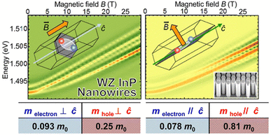
The figure on the left shows the coutor plots of the magneto-PL spectra of WZ InP NWs grown by SAE. The quantitative analysis of the diamagnetic shift of the different transitions observed lead to the determination of the electron and hole effective mass values reported in the tables. The values of the carrier mass clearly depend on the direction of motion in the nanowires. More details can be found in this link (Nano Letters).
|
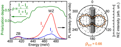
The effects of magnetic field on NWs was investigated also in InGaAs WZ NWs. These NWs show emission with a record 90% degree of polarization, as shown in the figure on the right.
Like InP WZ NWs, InGaAs WZ NWs show marked anisotropic electronic properties resulting into different values of the exciton reduced mass depending on the direction of motion. In addition, the WZ phase is apparent from the sizable dichroism of the PL intensity, as we reported in the ACS Nano. |
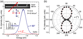
(a) PL spectra recorded under linear polarization filtering showing that emitted light is mianly polarized orthogonal to the NW c axis in agreement with the WZ phase. (b) PL intensity polar plot (click on figure to know more).
|
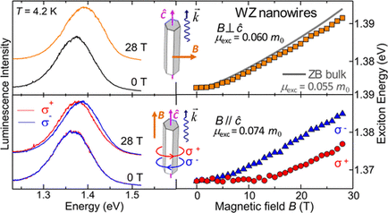
Left. PL spectra at different magnetic fields and for different field orientations recorded on InGaAs WZ NWs. Right. Exciton diamagnetic shift for the different field geometry employed.
|
Another largely investigated WZ NW system is represented by GaAs. Zincblende GaAs, along with Si, is the most investigated semiconductor. However, in the case of WZ GaAs NWs, even the band gap energy value and the conduction band structure are still debated.
We have recently provided the answer to a long discussed issue about the correct ordering of the conduction band states in WZ GaAs, namely Gamma7 character of the CB minimum. This has important consequences for the transport and photovoltaics applications of GaAs WZ NWs. The figure below (extracted from a work published in Nano Letters).
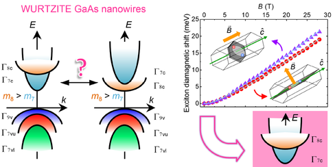
Left. Conjectured condution band structure for WZ GaAs NWs. Right. Diamagnetic shift data providing the right band order.
