
Optical Spectroscopy of Nanostructured Materials lab
Aim and equipment
The capability of modifying the physical properties of elemental and compound semiconductors through deliberate incorporation of foreign atoms into the crystal has led to the birth of modern electronics and optoelectronics. Improved performance and multifunctionality of devices have paralleled the progress achieved in the synthesis and engineering of new materials and in the control and modification of their physical properties at nanometre scale lengths. In particular, the synthesis of nanostructured semiconductors is incessantly boosting the number of solutions and the degree of flexibility available for large integration processes in electronics and photonics.
In our group, we address the electronic properties of novel semiconductor materials and nanostructures by investigating the emission and absorption of light in these systems. This can be accomplished by the use of several instruments and devices that excite materials and analyse spectrally and spatially subsequent light emission/absorption.
The following research topics are presently studied in our group (please follow the links for more information): semiconducting nanowires, nanostructures and photonics, two-dimensional materials, and hydrogen in novel materials.
Next, the main instrumentation available in our group is shown and briefly described.
The members of the Optical Spectroscopy of Nanostructured Materials Laboratory have decades of experience in the optical characterization of semiconductor materials and nanostructures. The lab is equipped with state-of-the-art facilities for optical spectroscopy, including:
|
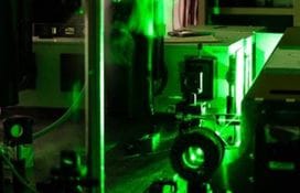
Diffused beam generated by a frequency-doubled Nd:YVO4 laser, with wavelength 532 nm and maximum power = 8 W.
|
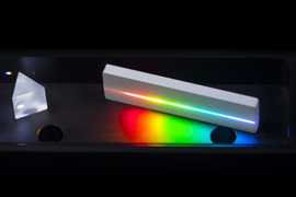
Emission from a Supercontinuum laser spanning over the wavelength range from 500 to 2200 nm (click on picture for more details).
|
- Double (0.75 m) and single (0.16, 0.3, and 1 m) monochromators.
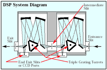
Double 0.75 m monochromator equipped with grating allowing detection from 350 to 3000 nm (click on figure for more details).
|
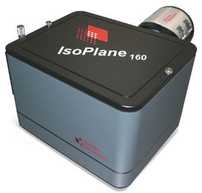
Single 20 cm monochromator featuring f/3.88 optics and a unique astigmatism-corrected optical design (click on figure for ore details).
|
|
Liquid-nitrogen cooled Si CCD (350-1000 nm) and InGaAs array (800-1700 nm) (click on figure for more details).
|
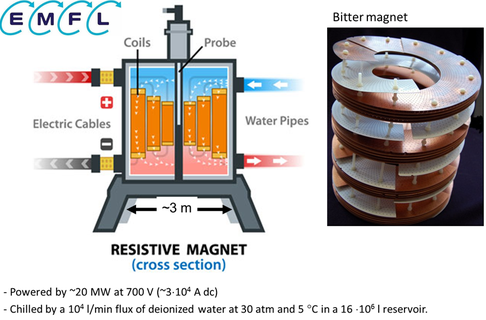
Schematic of the 33 T resistive Bitter magnet at the EMFL in Nijmegen. The Bitter magnet solenoid is shown on the right; up to 40 kA dc current flows on the magnetic helix.
|
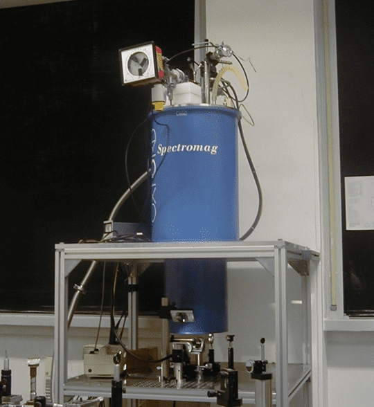
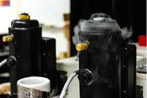
Superconducting magnet (maximum field 14 T) operating at liquid He temperature.
|
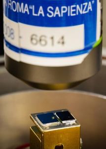
Zoom-in of the sample area, which is mounted on a x-y piezo-electric stages allowing for spatial resolution better than 100 nm. The laser can be focussed down to the diffraction limit dictated by the objcetive NA and laser wavelegnth. |
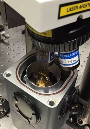
Sample chamber of a closed-cycle low-vibration cryostat with spatial resolution <100 nm coupled to confocal micriscope for single-nanostructure PL measurements (click on figure for details).
|
- Very recently we also designed and built a setup for photon correlation measurements (both pulsed and CW), which gave us the ability to fully characterize the performance of the investigated nanostructures as single- and entangled-photon emitters.
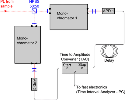
Sketch of the set-up for photon-correlation measurements. Photons are split toward two monochromator and time coincidences are recorded.
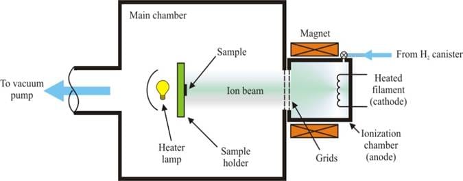
Detail of the Kaufman source employed for hydrogen irradiaton. The electrons ejected dissociate H molecules and the grid system focus H+ ions on the sample suitable heated and electrically grounded.
|
Low-energy (1-500 eV) Kaufman source for H (and light elements, such as He) implantation.
|
