Two-dimensional materials
Following the tremendous development of graphene over the past ten years, a lot of research interest has been attracted by atomically thin two-dimensional materials, such as topological insulators and transition metal dichalcogenides, TMDs, of the form MX2, where typically M=Cr, Mo, or W and X=S, Se, or Te). TMDs are layered semiconductors with strong in-plane bonding and weak out-of plane interaction that enables mechanical exfoliation into few or even a single layer, just as graphene can be obtained from graphite. At variance with graphene that lacks an energy band gap and therefore has somehow limited optical use, TMDs exhibit remarkable optical properties stemming from their unique electronic structure. Figure 1 shows a schematic representation of a typical MX2 bulk structure. MX2 single layers are weakly held together by van der Waals forces to form the bulk crystal. Each layer has a plane of hexagonally arranged metal atoms sandwiched between two planes of hexagonally arranged dichalcogen atoms. The metal atoms have a 6-fold coordination symmetry stemming from the hybridization between the X pz-orbitals and the M d-orbitals. Several polytypes are possible depending on the stacking order and metal atom coordination (as an example, Figure 1 shows the 2H, namely the polytype with hexagonal symmetry).
Transition-metal dichalcogenides are indeed an emergent class of semiconducting materials with extraordinary opto-electronic properties when reduced to few layers. In the monolayer limit, they emit light efficiently in the visible/infrared region and their flexibility and robustness allow to exploit mechanical deformations to change their inherent properties.
Transition-metal dichalcogenides are indeed an emergent class of semiconducting materials with extraordinary opto-electronic properties when reduced to few layers. In the monolayer limit, they emit light efficiently in the visible/infrared region and their flexibility and robustness allow to exploit mechanical deformations to change their inherent properties.
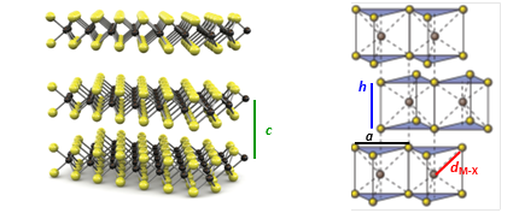
Figure 1. Left: Three-dimensional schematic representation of a typical MX2 structure, with the chalcogen atoms (X) in yellow and the metal atoms (M) in grey. Right: Schematics of the structural 2H polytype (hexagonal symmetry, two layers per repeat unit, trigonal prismatic coordination). a indicates the lattice constant, dM-X is the bond length, h is the sheet thickness, and c is distance between two adjacent in-plane chalcogenide atoms.
We are presently studying the effects of hydrogen incorporation in these fascinating materials (thesis available).
We have recently demonstrated a novel route toward the strain-patterning of TMDs based on the effects of low-energy proton irradiation on the structural and electronic properties of bulk WS2, WSe2, WTe2, MoS2, MoSe2 and MoTe2. Suitable irradiation conditions trigger the production and accumulation of H2 just beneath the first X-M-X basal plane. As a consequence of the balance between the gas expansion, the van der Waals forces holding the S-W-S planes together and the material’s elastic properties, localized swelling of just one ML takes place, resulting in the formation of atomically-thin and spherically-shaped domes see Figure 2. The domes cage highly-pressurized H2 and are durable thanks to the impermeability to H2 of TMD MLs, as reported in Advanced Materials.
We have recently demonstrated a novel route toward the strain-patterning of TMDs based on the effects of low-energy proton irradiation on the structural and electronic properties of bulk WS2, WSe2, WTe2, MoS2, MoSe2 and MoTe2. Suitable irradiation conditions trigger the production and accumulation of H2 just beneath the first X-M-X basal plane. As a consequence of the balance between the gas expansion, the van der Waals forces holding the S-W-S planes together and the material’s elastic properties, localized swelling of just one ML takes place, resulting in the formation of atomically-thin and spherically-shaped domes see Figure 2. The domes cage highly-pressurized H2 and are durable thanks to the impermeability to H2 of TMD MLs, as reported in Advanced Materials.
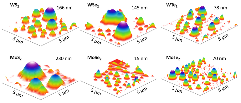
Figure 2. 3D atomic force microscopy (AFM) images of 5 µm × 5 µm areas acquired on 6 different
TMDs, showing the formation of domes in all the samples. The maximum height reached by
the domes is also written for each panel.
Structural and optical characterizations confirm that these domes are typically one ML-thick and contain H2 at pressures in the 10-100 atm range, depending on their size. Such high pressures induce strong and complex strain fields acting on the curved X-M-X planes. The single-layer nature of the domes is witnessed by their high optical efficiency as shown in Figure 3, displaying two optical microscope images under white and laser light illumination.
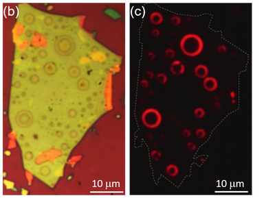
Figure 3. (b) Optical image of a WS2 flake, where many domes formed after proton-irradiation. (c) Laser-excited red luminescence coming from the same flake shown in panel (b).
The characteristic ring-like behaviour is due to the change of the strain-induced character of the band gap from direct to indirect.
The domes’ morphological characteristics can be tuned by lithographically controlling the area of the sample basal plane participating in the hydrogen production process (see Figure 4). This results in the unprecedented fabrication of robust domes with controlled position/density and sizes tunable from the nanometer to the micrometer scale, that, by virtue of their inherently strained nature and geometry, might prompt a variety of applications (Advanced Materials Interfaces, in press).
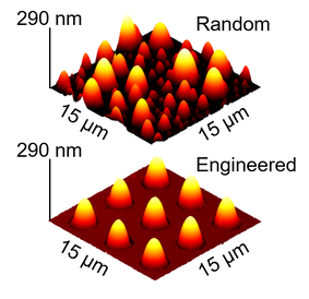
Figure 4. Formation of random and patterned arrays of MoS2 domes. (top) AFM image of a 15×15 µm2 area of a proton-irradiated MoS2 flake. The largest dome has a footprint diameter about 1 µm formed on the flake surface following the irradiation process. The aspect ratio for these domes varies between about 0.14 and 0.18. (bottom) Same for MoS2 flakes patterned with an 80-nm-thick mask with openings of size S = 3 µm. The diameter of the domes is in this case determined by the size of the opening, and higher aspect ratios (0.22) with respect to the random domes are obtained.
The non-trivial strain fields hosted by the domes feature sufficiently high tensile in-plane strains (about 2.7% in WS2-ML) turning the deformed WS2 monolayer from a direct band gap material into an indirect-gap one. This general behavior, common to other TMDs—like MoS2 and WSe2—must be considered when 2D crystal are to be employed in flexible optoelectronic devices, or possibly exploited for the observation of quantum many-body effects involving long-lived k-space indirect excitons. Thiere results are reported in Physical Review Research as a Rapid Communication.
Figure 5 summarizes the strain-induced band gap transition in WS2.
Figure 5 summarizes the strain-induced band gap transition in WS2.
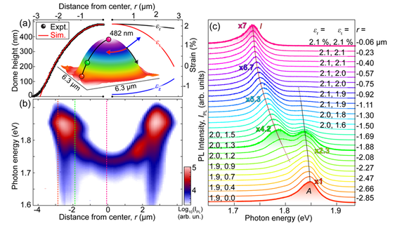
Figure 5. Height profile of a WS2 dome measured by AFM (black dots; the AFM image is shown as inset), and computed by FEM calculations (solid red line). Right: Dependence along the dome radius of the strain tensor components, represented as color-coded arrows in the inset. The three dots (purple: top; green: intermediate; orange: edge) correspond to the positions displayed as dashed lines in (b) and to the shadowed spectra in (c). (b) Micro-PL scan along a diameter of the dome displayed in (a), performed at 297 K. The horizontal axis indicates the laser spot position with respect to the dome center, the vertical axis indicates the emitted photon energy. The base-10 logarithm of the micro-PL intensity is shown in a false color scale. (c) Normalized emission spectra of the dome as the laser spot is scanned from the dome’s left edge (bottom) to its apex (top). Spectra are labeled with the laser spot position and with the values of the radial and circumferential strain components. The solid lines follow the energy shift of the direct (A, black line) and indirect (I, red line) exciton transition.
